- Home
- >
- Applications
- >
- Electronics
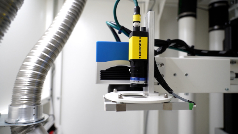
Electronics
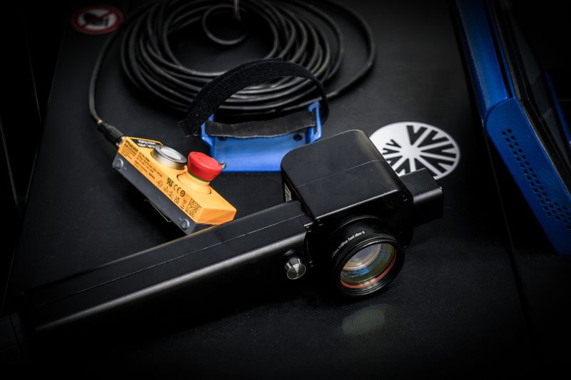
The electronics and renewable energy sector is among the most dynamic and fastest growing. The laser is used extensively for the processing of semiconductors, printed circuits, electronic components, solar panels and batteries. The systems suitable for this purpose, to meet industry standards, must combine high precision with a very high process speed.
SEMICONDUCTORS
- processing of silicon wafers: Scribing P1, P2, P3, Dicing and marking.
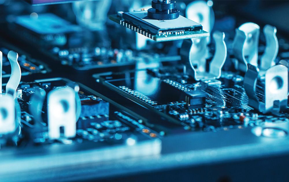
PCB PROCESSING
- Drilling of blind vias and throug holes vias in rigid and flexible PCBs. PCB materials, such as RCC, FR4, FR5, polyimide etc.
- Cutting edges and parts in rigid and flexible PCBs and coverlayers. Clean and high precision cuts with minimum cutting width in various PCB materials, such as RCC, FR4, FR5, PTFE, CEM, polyimide etc.
- Laser Structuring: geometric processing of the upper copper layer of the PCB with minimal thermal damage to the underlying materials.
- Depaneling: clean and stress-free cutting on populated rigid and flexible PCBs.
- SMT screen printing foils (stainless steel, polymeric supports): creation of stencil openings on sheets from 20 μm to 1 mm with the possibility of defining the geometric properties.
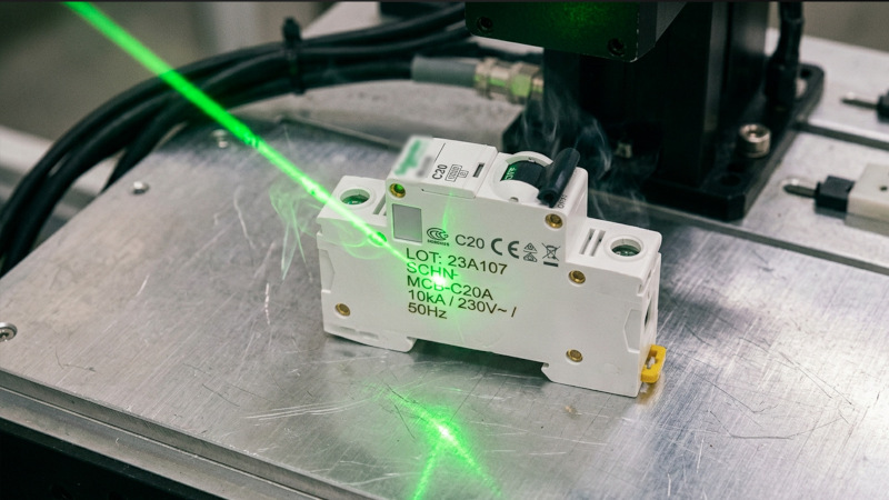
ENERGY
- Thin film photovoltaic cells: Scribing P1, P2, P3, Cell edge cleaning
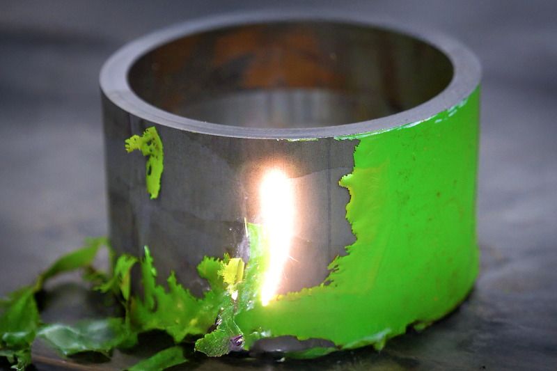
- Batteries: Welding, Sealing, Cutting and Wire stripping terminals
- LED bulbs: Scribing, Lift off, marking